Following are the interactive versions of the circuits used in the document:
Logic gates are used in a digital circuit to perform various operations and control flow in the circuit. There are various logic gates from basic to complex. Basic logic gates include, AND, OR, NOT, NAND, NOR, XOR, XNOR. Basic logic gates can be used to create other logic gates, like combining AND and NOT gives, NAND.
Basic Logic Gates
Following are the basic logic gates:
NOTANDORNANDNORXORXNOT
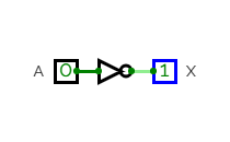
NOT gate
Truth table for NOT gate:
| 0 | 1 |
| 1 | 0 |
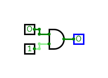
AND gate
Truth table for AND gate:
| 0 | 0 | 0 |
| 0 | 1 | 0 |
| 1 | 0 | 0 |
| 1 | 1 | 1 |
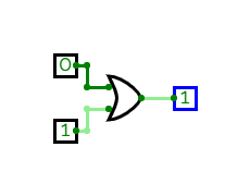
OR gate
Truth table for OR gate:
| 0 | 0 | 0 |
| 0 | 1 | 1 |
| 1 | 0 | 1 |
| 1 | 1 | 1 |
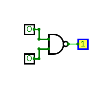
NAND gate
Truth table for NAND gate:
| 0 | 0 | 1 |
| 0 | 1 | 1 |
| 1 | 0 | 1 |
| 1 | 1 | 0 |
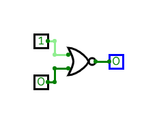
NOR gate
Truth table for NOR gate:
| 0 | 0 | 1 |
| 0 | 1 | 0 |
| 1 | 0 | 0 |
| 1 | 1 | 0 |
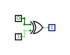
XOR gate
Truth table for XOR gate:
| 0 | 0 | 0 |
| 0 | 1 | 1 |
| 1 | 0 | 1 |
| 1 | 1 | 0 |
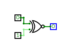
XAND gate
Truth table for XAND gate:
| 0 | 0 | 1 |
| 0 | 1 | 0 |
| 1 | 0 | 0 |
| 1 | 1 | 1 |
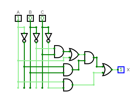
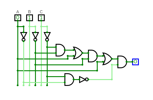
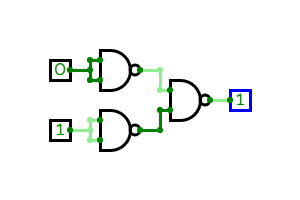
Example 1: Draw logic circuit for .
Method 1: Using direct lines, the circuit can be drawm as:
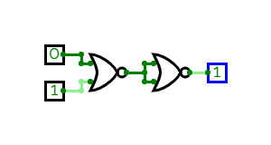
Method 2: Using parallel lines, the circuit can be drawn as:
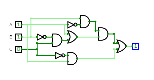
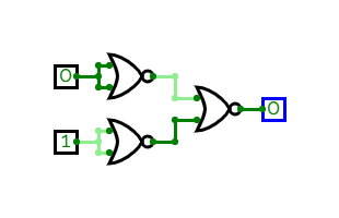
Example 2: Draw logic circuit for
Following is the logic circuit for the above operation:
Universal Gates
NAND and NOR gates are called universal gates because they can be used to form any other gates.
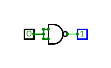
Using NAND gate
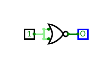
NOT gate
AND gate
OR gate
Using NOR gate
NOT gate
AND gate
OR gate
Circuit Conversion
Using NAND only
NAND gate being an universal gate, can be used to convert all gates in a circuit to it, i.e., all gates within the circuit can be converted into NAND gate. The circuit thus will be made of only NAND gate. The steps to do so are:
- For
ANDgates, theNOTwill be placed infront of the gate towards the output. - For
ORgates, theNOTs will be placed behind the gate from the inputs. - All
NOTs infront ofANDgate will be cancelled. Consequetively anyNOTbehindORgate will be cancelled. - The circuit must be balanced. Any
NOTadded to the circuit must be countered with anotherNOTin the same line.
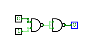
Example 3: Construct, using NAND gates only.
Circuit using normal gates:
In the above circuit, NOT gates from the main line will be converted into, NAND-NOT circuit. The AND gate operating , will have a NOT infront of it, which will be countered by the NOT behind the frontal OR gate. The frontal OR's second input coming from will be changed to in order to counter for the NOT behind the OR gate. The AND gate operating , will have a NOT infront of it, and since it is connected further to an AND gate, a NOT gate will be added to balance the circuit. The final OR will receive two NOTs from the preceeding ANDs, and give the final result.
Final circuit using NAND gates only:
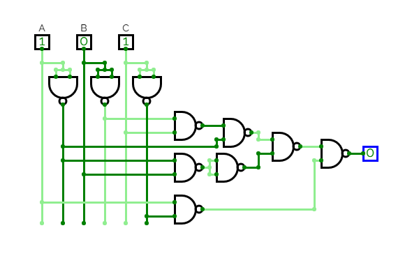
Exercise 1
-
Draw a circuit for , using
NANDgates only. -
Draw a circuit for the following using
NANDgates only: