Following are the interactive versions of the circuits used in the document:
Combinational circuits are very well known components in digital electronics which can provide output instantly based on the current input. Unlike sequential circuits, a combinational circuit listens for input signal and and generates output no matter what is the past input or state as it has no feedback or memory component. It only cares about present input and state.
Multiplexer
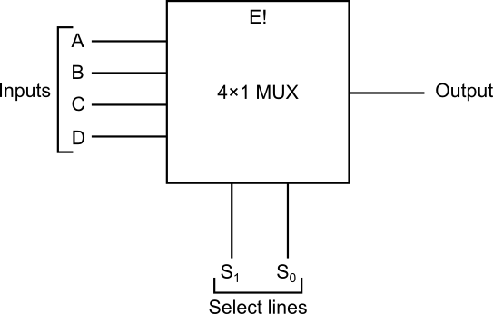
A multiplexer is a combinational circuit that selects one digital information from several sources, and sends it on a single output line.
It is also called data selector.
Block diagram
Truth table
| Output | ||
|---|---|---|
| 0 | 0 | A |
| 0 | 1 | B |
| 1 | 0 | C |
| 1 | 1 | D |
Construction
- It has input lines.
- It has select lines.
- It has only one output line.
- or stands for low input enable line.
- Only one of the input line gets selected depending upon the select lines as shown in the truth table.
Circuit diagram
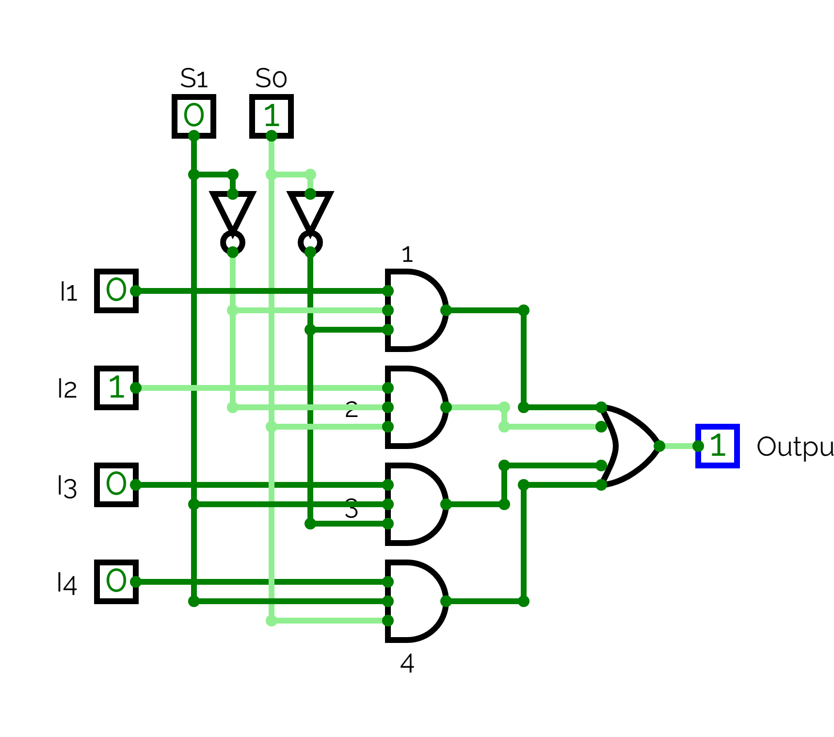
Working
When, , and :
ANDgate 1 =ANDgate 2 =ANDgate 3 =ANDgate 4 =
Finally the OR gate = . Hence input is selected. Similarly in other cases their respective inputs are selected.
Applications
- Data routing
- Logic function generator
- Parallel to serial convertor
Demultiplexer
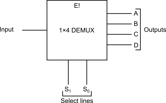
It is a combinational circuit that receives information on a single input line and transmits the same information over one of several () output lines.
It is also called data distributor.
Block diagram
Truth Table
| Output line | ||
|---|---|---|
| 0 | 0 | A |
| 0 | 1 | B |
| 1 | 0 | C |
| 1 | 1 | D |
Construction
- Has single input line.
- It has select lines.
- It has output lines.
- It has one active low enabled line.
Circuit diagram
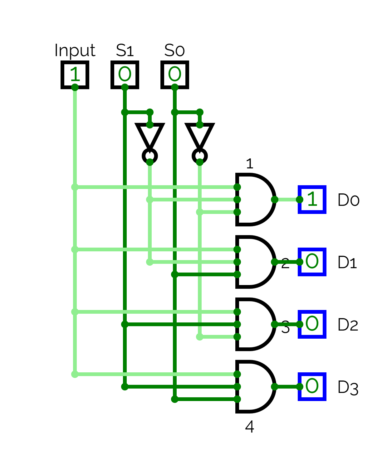
Working
When, , and :
ANDgate 1 receivesANDgate 2 receivesANDgate 3 receivesANDgate 4 receives
Hence, line is selected. Similarly the other lines are selected for their respective combinations of and .
Applications
- Serial to parallel convertor
- Seperates signals from mixed signals
- Used in communication system
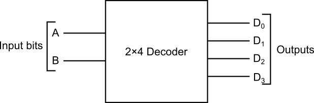
Decoder
A decoder is a logic circuit that converts -bit binary inputs into output lines, such that each output line will be activated for only one of the possible combination of inputs.
Block diagram
Truth table
| 0 | 0 | 1 | 0 | 0 | 0 |
| 0 | 1 | 0 | 1 | 0 | 0 |
| 1 | 0 | 0 | 0 | 1 | 0 |
| 1 | 1 | 0 | 0 | 0 | 1 |
Circuit diagram
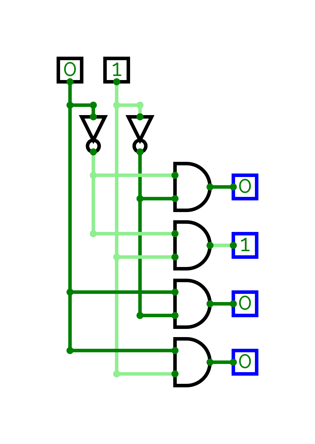
Working
When, , and :
ANDgate 1 receivesANDgate 2 receivesANDgate 3 receivesANDgate 4 receives
Thus, the line gets activated and the rest are all deactivated. Similarly all other lines get active for their respective combination of inputs.
Application
- Data demultiplexing
- Digital display
- Digital to analogue convertor
- Memory adressing
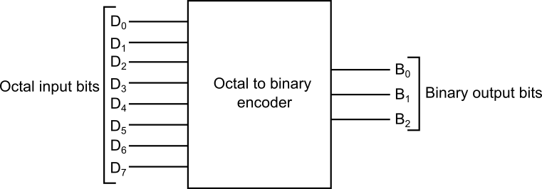
Encoder
An encoder is a combinational logic circuit that converts an active input signal into a coded output signal. It encodes one of the active input to a coded binary output with -bits.
We will consider octal to binary encoder circuit for the explanation:
Block diagram
Truth table
| 1 | 0 | 0 | 0 | 0 | 0 | 0 | 0 | 0 | 0 | 0 |
| 0 | 1 | 0 | 0 | 0 | 0 | 0 | 0 | 0 | 0 | 1 |
| 0 | 0 | 1 | 0 | 0 | 0 | 0 | 0 | 0 | 1 | 0 |
| 0 | 0 | 0 | 1 | 0 | 0 | 0 | 0 | 0 | 1 | 1 |
| 0 | 0 | 0 | 0 | 1 | 0 | 0 | 0 | 1 | 0 | 0 |
| 0 | 0 | 0 | 0 | 0 | 1 | 0 | 0 | 1 | 0 | 1 |
| 0 | 0 | 0 | 0 | 0 | 0 | 1 | 0 | 1 | 1 | 0 |
| 0 | 0 | 0 | 0 | 0 | 0 | 0 | 1 | 1 | 1 | 1 |
Circuit diagram
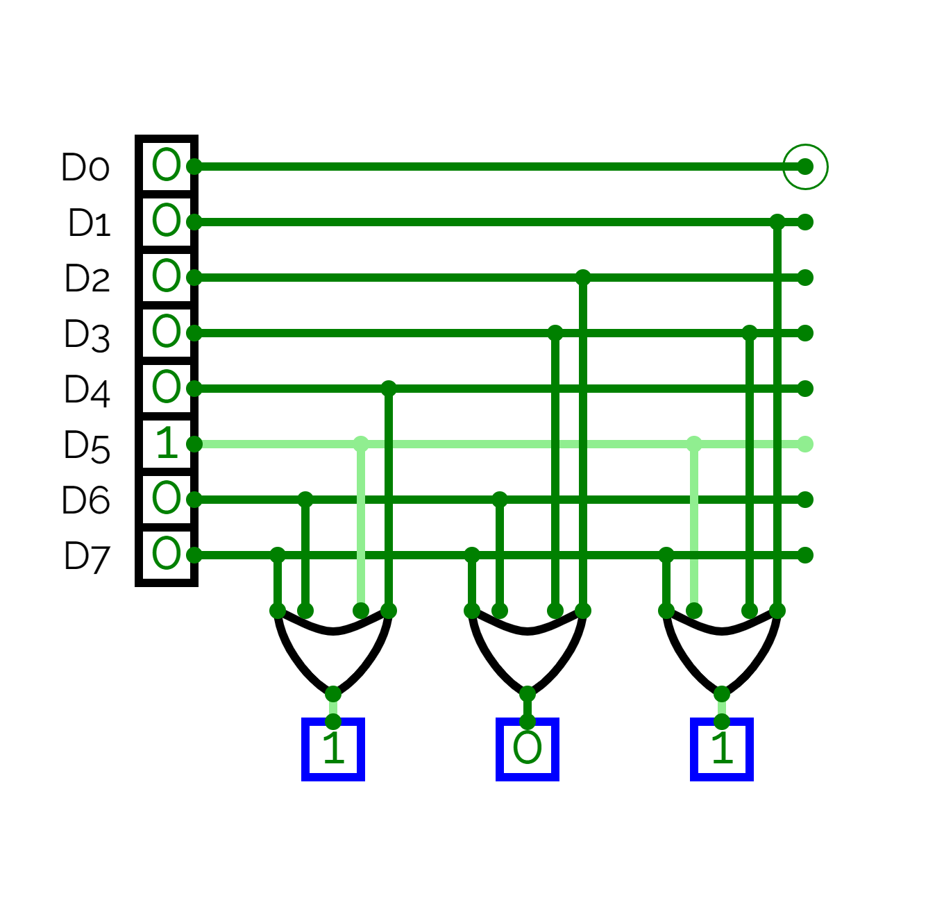
Working
- It has 8 input lines. Only one is active at a time.
- It has 3 output lines which generates binary code for the octal number that is active.
- From the above truth table must be 1 whenever the input , or , or , or is high. Thus we can say the following:
- For example: if is active,
ORgates will have 101 as output. - Similarly other cases show different outputs, for their respective inputs.